Technology R&D

Release date:2025-02-13

Intelligent Enabling Technology

Continuous Water Quality Monitoring Technology

Continuous water quality monitoring technology and intelligent transformation and upgrading of production water management. Smart water quality monitoring technology helps the metal processing industry achieve zero discharge water exceeding the standard and reduce carbon emissions by 10%.


Environmental (E)

Social (S)

Economic (E)

Zero exceedance of metal processing effluent standards to prevent environmental pollution.

Reducing manual meter reading and hazardous environment operation time by 50%, ensuring employee work safety.

Internal controls comply with environmental regulations to prevent effluent exceeding standards that could lead to work suspension.


Solutions

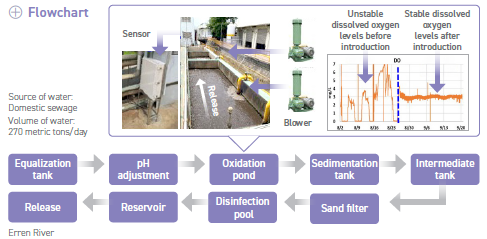
Developing long-lasting anti-biofilm water quality sensing technology and introducing smart low-carbon water quality monitoring technology. By using water quality sensors to feedback and control the flow ratio of high-concentration waste liquid and the aeration volume of the biological pool, zero exceedance in effluent discharge standards has been achieved and carbon emissions from water treatment have been reduced by 10% per plant.

Technology Application

ž   By developing anti-biofilm technology, the rate at which microorganisms and contaminants adhere to water quality sensors in sewage is mitigated, achieving accurate continuous measurement and extending the manual maintenance cycle by more than four times.

ž   By developing a composite water quality sensing system technology, it is possible to provide continuous six-in-one sensing of copper ions, chemical oxygen demand, suspended solids, pH, conductivity, and water temperature. Additionally, seven types of pattern recognition for water quality signal have been developed to assist in automated water quality anomaly warnings, eliminating the burden of manual interpretation.

Achievements

ž   Assisted leading manufacturers of metal processed products (such as server guide rails and automotive fasteners) in implementing smart low-carbon water quality monitoring technology. Supported the mixing and homogenization of high-concentration waste liquid, aeration control in biological oxidation ponds, and continuous water quality monitoring before discharge. Achieved zero exceedance of effluent standards and reduced carbon emissions from water treatment by 10% per plant.

ž   Assisted the Environmental Protection Bureaus of Taichung City Government and Kaohsiung City Government in continuous monitoring of urban river water quality to prevent public panic caused by fish kills; assisted high-density aquaculture operators in monitoring water quality changes after feeding to avoid excessive accumulation of organic matter in ponds, which could lead to accidental losses.

水流

Panel Business Transitioning to Semiconductor Packaging - FOPLP Panel-level Packaging

Revitalizing the existing assets of panel factories to create a production value of NT$100 billion and increasing international competitiveness.


Environmental (E)

Social (S)

Economic (E)

Revitalized old-generation panel production lines by transforming them into semiconductor packaging lines. With 70% of the existing panel production lines reusable, environmental impact has been reduced

Assisted Innolux's Southern Taiwan Science Park (STSP) Plant 1 in becoming the world's first production line for panel-level semiconductor packaging transformation, retaining more than 1,000 production line employees

Facilitated Innolux Corporation to drive related industry investments amounting to several billion New Taiwan dollars, with the estimated output value expected to reach a scale of NT$100 billion


Solutions

Utilizing the large-scale copper electroplating technology developed by the Institute, we assisted domestic equipment manufacturers in developing large-size, high-uniformity copper electroplating equipment. Additionally, we developed the panel warpage suppression technology and introduced it to Innolux, aiding in the establishment of a high yield rate semiconductor packaging copper wire process.

Technology Application

ž   Due to the panel manufacturers' lack of experience in critical electroplating processes during their transition to semiconductors, they have collaborated with domestic electroplating equipment manufacturers to fill the technical gaps.

ž   Since panel-level packaging involves a thick film process compared to the original display manufacturing, controlling warping is even more challenging. Therefore, the stress simulation technology originally developed for flexible displays is utilized to assist panel manufacturers in predicting substrate warping values.

ž   Utilizing the G2.5 pilot line to actually verify the control of substrate warping and the photomask-free redistribution layer technology so as to meet the future demands of advanced panel-level IC packaging.

Achievements

ž   Assisted Innolux in achieving mass production-level yield rates for their panel-level semiconductor packaging production line.

ž   Drove the development of domestic upstream materials and equipment, and took the lead in strategic deployment.

ž   The patent portfolio has been recognized and licensed to key industry players such as Innolux and TSMC, thereby strengthening international competitiveness.


群創

Contact Us

※ TAll fields marked with an asterisk (*) must be completed.

Please check the box to agree to the Legal Statement。

We record cookie information to provide personalized content and optimize your user experience. By continuing to browse this website, you agree to our use of cookies. For more information on privacy protection, please refer to our Privacy Policy